NEWS
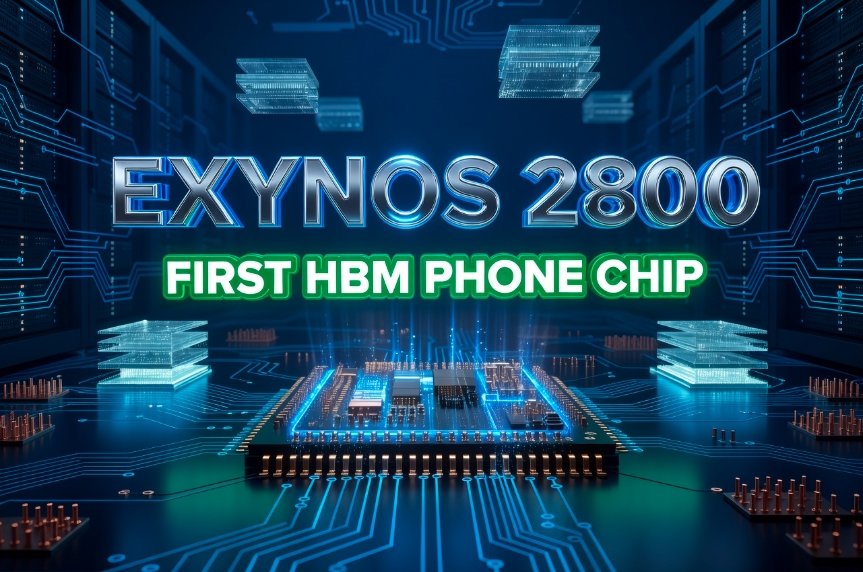
Samsung Exynos 2800 Could Be First Phone Chip With HBM
What if your phone could run powerful AI without ever pinging a server? Samsung is reportedly building the technology to make that happen, and it could be a world first for smartphones.
The company is developing new packaging technology to bring High Bandwidth Memory to mobile chips, possibly starting with the Exynos 2800. If it works, Samsung could beat Apple, Huawei, and every other chipmaker to this milestone.
Why On-Device AI Is Still Hitting a Wall
Most people do not realize this, but when your phone answers a complex AI query, the actual heavy lifting often happens in a remote data center, not on your device.
Your request travels to the cloud, gets processed, and the answer comes back to you. It usually feels instant. But it is not true on-device AI, and it carries real concerns around privacy, latency, and connectivity.
The core reason on-device AI remains limited on smartphones is not just processing power. It is memory bandwidth, which controls how fast data can be fed into the chip for AI tasks.
Traditional mobile DRAM uses copper wire bonding and is capped at 128 to 256 I/O terminals. This causes significant signal loss and keeps bandwidth far too low for demanding AI models to run at their full potential locally.
High Bandwidth Memory, or HBM, solves this exact problem. It is the same memory that powers AI data centers and the world’s fastest GPU servers today. The challenge is that nobody has managed to fit it inside a thin smartphone, until now.
Samsung Exynos 2800 HBM mobile chip on-device AI performance
The Clever Packaging Tech Samsung Is Quietly Engineering
According to a report from Korean publication ETNews, Samsung is actively developing a new packaging method called Vertical Copper Post Stack, or VCS, designed specifically to bring HBM to mobile devices.
The method stacks DRAM dies in a staircase-like arrangement, with copper pillars filling the gaps between each layer. Samsung has dramatically increased the aspect ratio of those copper pillars from the existing 3-5:1 ratio all the way up to 15:1 to 20:1, which is a significant engineering leap forward.
There is a structural risk here. When copper pillar diameters shrink below 10 micrometers, they can bend or completely snap under pressure.
Samsung’s solution is Fan-Out Wafer Level Packaging, or FOWLP, which extends the copper wiring outward to provide structural stability and prevent breakage. It also increases the number of I/O terminals, contributing to an estimated 30 percent increase in total bandwidth. FOWLP is already used on the Exynos 2600, so Samsung is building on packaging technology it already has proven manufacturing experience with.
Here is what Samsung’s new packaging approach could deliver compared to what exists today:
- Current mobile DRAM: Limited to 128-256 I/O terminals with notable signal loss and capped bandwidth
- VCS copper pillar tech: Aspect ratio pushed from 3-5:1 to 15:1-20:1 for much denser memory stacking
- FOWLP structural support: Prevents fragile pillars from breaking and significantly boosts I/O terminal count
- Expected bandwidth gain: 15 to 30 percent more bandwidth and over 1.5x memory stack capacity
Exynos 2800 Is Already Samsung’s Most Ambitious Chip Yet
The HBM packaging story is just one piece of a much bigger picture forming around the Exynos 2800, codenamed internally as “Vanguard.”
Samsung has reportedly set a target to complete the chip’s tape-out before the end of 2026. Tape-out is the final design phase before the chip moves into full-scale production. The Exynos 2800 is expected to power the Galaxy S28 series in early 2028 and will use Samsung Foundry’s third-generation 2nm process called SF2P+, which delivers improved performance and power efficiency over the current generation.
Unlike previous Exynos chips that relied on AMD for graphics, the Exynos 2800 is reportedly set to debut a fully in-house GPU architecture, a move that would cut Samsung’s dependence on external partners entirely.
Reports also suggest Samsung may incorporate custom in-house CPU cores as well, making the Exynos 2800 the most self-sufficient chip the company has ever built. Here is what the full package reportedly looks like:
- Samsung’s SF2P+ third-generation 2nm process with better power efficiency and performance density
- A fully in-house GPU architecture, breaking from the current AMD-based Xclipse design
- Possible custom CPU cores developed entirely by Samsung System LSI
- HBM support through VCS and FOWLP packaging for significantly boosted memory bandwidth
Apple is also reportedly exploring mobile HBM for its 2027 anniversary iPhone, with both Samsung Electronics and SK Hynix developing competing technologies for the Cupertino giant. SK Hynix is working on a method called Vertical Wire Fan-Out, or VFO, while Samsung pursues VCS. The race is already on, and the company that gets there first will own a defining claim in mobile chip history.
A Business Win That Goes Well Beyond the Chip
This story is not just about technology. It is about strategy, and the numbers behind it are staggering.
Samsung has already started mass production of HBM4, its latest generation of high-bandwidth memory built for AI data centers. HBM4 delivers up to 3.3 terabytes per second of memory bandwidth per stack, which is 2.7 times higher than the previous HBM3E generation. Samsung expects its total HBM sales to more than triple in 2026 compared to 2025.
If Samsung successfully brings HBM to smartphones and other chipmakers follow its lead, demand for Samsung’s memory could surge across two massive and separate markets at the same time.
There is another angle worth noting here. The AI industry’s relentless demand for data center HBM has put enormous pressure on global memory production. A viable mobile HBM market could help Samsung better utilize its growing production capacity and reduce overall supply strain. Industry analysts also point out that Samsung is one of the very few companies in the world that controls both chip design and memory production in-house. That gives it a hardware integration depth that rivals like Qualcomm and MediaTek simply cannot replicate on their own.
When Will This Actually Reach Your Hands
The Exynos 2700 is on track for mass production later this year and is expected to power the Galaxy S27 series in 2027. The Exynos 2800 with all its rumored upgrades would then follow for the Galaxy S28 in early 2028, placing the earliest possible HBM-equipped Samsung phone at least two years away.
Samsung has not officially confirmed any of the reported details around the Exynos 2800 or its HBM roadmap. The technology is still in active development, and there is a real possibility that mobile HBM could slide past the Exynos 2800 and debut instead with the Exynos 2900 if engineering challenges cause delays.
Even the possibility of HBM arriving in a consumer smartphone by 2028 represents a turning point for mobile AI, and the engineering work happening right now is what will determine how fast that future arrives.
Samsung’s push to bring HBM to the Exynos 2800 is not just a spec upgrade. It is a signal that the smartphone industry is rethinking what a phone is capable of from the ground up. Real-time AI translation, private on-device generative AI, faster and smarter photography processing without cloud dependency, all of it becomes far more achievable once memory bandwidth stops being the bottleneck. The company that cracks this first will set the rules for mobile AI for years to come. Are you excited about the idea of true on-device AI in your next Samsung phone? Drop your thoughts in the comments below.

Revolut Targets a 2027 US Bank Launch After Its First Bid Collapsed

Helsing Hits an $18 Billion Valuation as Drone Doubts Persist

Fusion Cash and Bank Debt Define Europe’s €2.8 Billion Tech Week

Doctorsa Raises €1 Million and Opens Doctor Bookings to AI Agents
Michael Saylor’s Bitcoin Post Leaves Strategy’s Next Move a Mystery
The Windows Identifier That Caught a Hacker Cannot Be Turned Off

US Strikes Iran for a Third Time as Bitcoin Slips Below $64,000

Musk Brands Altman a ‘Scammer’ as Apple Sues OpenAI Over Trade Secrets

SK Hynix’s CEO Warns the RAM Shortage Will Outlast Its Record IPO

Bessent’s No-CBDC Applause Line Can’t Save the CLARITY Act

CLARITY Act Final Text Expected This Weekend as 60-Vote Hurdle Looms

Fed Minutes Cite AI Demand as Inflation Risk, Put a 2026 Hike Back on the Map

Kalshi Loses Major NY Prediction Markets Ruling to Judge Torres

Marker AI Writing Startup Lands $13M Seed Led by Index Ventures

Meta’s Muse Spark 1.1 Beats Rivals on Price, Trails on Coding

Dota 2 Esports World Cup 2026: Spirit Defends $2M Title In Paris

CS2 Premier Season 5 Lands With Cache and a C4 Damage Rework

Trump Calls Iran ‘Islamic Republic of Japan’ as Ceasefire Ends

Backrooms Returns to Theaters as the Everything Must Go Edition

The Furious Stages Action Like Combat Choreographed by Ants
-
 FINANCE1 month ago
Zcash Patched a Double-Spend Bug as ZEC Climbed 5%
-
 ENTERTAINMENT1 month ago
Steam Summer Sale 2026 Locks In June 25 to July 9 Dates
-
 NEWS2 months ago
Meta Adds AI Replies to Threads, But Users Can’t Block It
-
 FINANCE1 week ago
CLARITY Act Final Text Expected This Weekend as 60-Vote Hurdle Looms
-
 ENTERTAINMENT2 months ago
‘Widow’s Bay’ Review: Apple TV’s Sleeper Horror-Comedy Earns Its Fog
-
 ENTERTAINMENT1 month ago
Amazon Scraps Its Stargate Revival After a 20-Week Writers Room
-
 FINANCE5 days ago
Fed Minutes Cite AI Demand as Inflation Risk, Put a 2026 Hike Back on the Map
-
 FINANCE1 month ago
Citigroup Says ETF Outflows Drove Bitcoin’s Crash, Not Strategy’s Sale