
NEWS
QuantumDiamonds Opens Its First Munich Chip Inspection Bay
QuantumDiamonds opened its first Munich bay and locked a €76 million Chips Act grant, but the diamond tools still work in analysis labs.

QuantumDiamonds opened the first hall of its €152 million Munich plant on July 23, 2026, after Brussels cleared a Chips Act grant that covers half the site.
The Commission found the factory would not have been built in Europe without that money. The first commercial QDm.1 scanners were already running in failure-analysis labs in Sunnyvale, California, and Hsinchu, Taiwan.
Brussels Paid Half the Plant to Keep It in Munich
On June 23, 2026, the European Commission approved a €76 million German state-aid measure for QuantumDiamonds GmbH’s IPF-ATEST project, a direct grant from the federal economy ministry and the Free State of Bavaria. The file is the fourteenth such decision under the principles of the European Chips Act, after about €14.2 billion in earlier aid across member states, and the fifth project taken from Germany’s November 2024 call.
The arithmetic is blunt. Seventy-six million is 50% of the €152 million eastern Munich site the company announced on December 15, 2025. In its decision the Commission wrote that the aid has an incentive effect, because without public support the company would not carry out the investment in Europe.
That finding is the industrial fact inside the sovereignty speeches. The product is inspection gear for other people’s fabs, and the plant sits in Munich because the grant closed a funding gap the Commission accepted as proven.
THE MONEY BEHIND THE MUNICH SITE
| Use | Amount | Date |
|---|---|---|
| Production plant, eastern Munich | €152 million ($178 million) | Plan announced Dec. 15, 2025 |
| Direct grant, IPF-ATEST | €76 million | Cleared June 23, 2026 |
| Series A equity, World Fund lead | €15 million | Closed July 9, 2026 |
| Grant plus equity package | €91 million | July 9, 2026 |
On July 9 the company closed an €15 million equity round led by World Fund, with Bayern Kapital and existing backers IQ Capital, Earlybird, First Momentum, UnternehmerTUM, Creator Fund, Onsight Ventures, and angels. Combined with the grant, that is the €91 million package. QuantumDiamonds said it is the only startup awarded manufacturing funding under the Act, putting it in a cohort that already includes GlobalFoundries and Carl Zeiss.
Kevin Berghoff, chief executive and co-founder, said the round was a step toward putting quantum sensing into fabs worldwide, and that leading chipmakers now treat the tools as a way to solve yield problems current systems cannot. The firm employed 70 people at the time and said it would more than double the engineering team over the following 12 months.
WHAT THE GRANT REQUIRES
- Priority orders: In a supply shortage the company must fulfil orders on a priority basis.
- Shared floor: Part of the site must be made available to early-stage firms, startups, and academic labs.
- Profit clawback: Project profits above current expectations are to be shared with Germany.
- Research ties: Collaborations with universities and research institutes must be strengthened.
- IPF track: The firm is applying for Integrated Production Facility under the Chips Act and has committed to the duties that status carries.
Daria Saharova, managing partner at World Fund, put Europe’s chip gap in two figures: the region uses around 20% of the world’s semiconductors and produces only 10%. She placed the company in a $104 billion equipment market. Those are investor lines. The Commission’s own test was narrower. Pay enough of the plant, or watch it leave.
The First Hall Came Up in Four Months
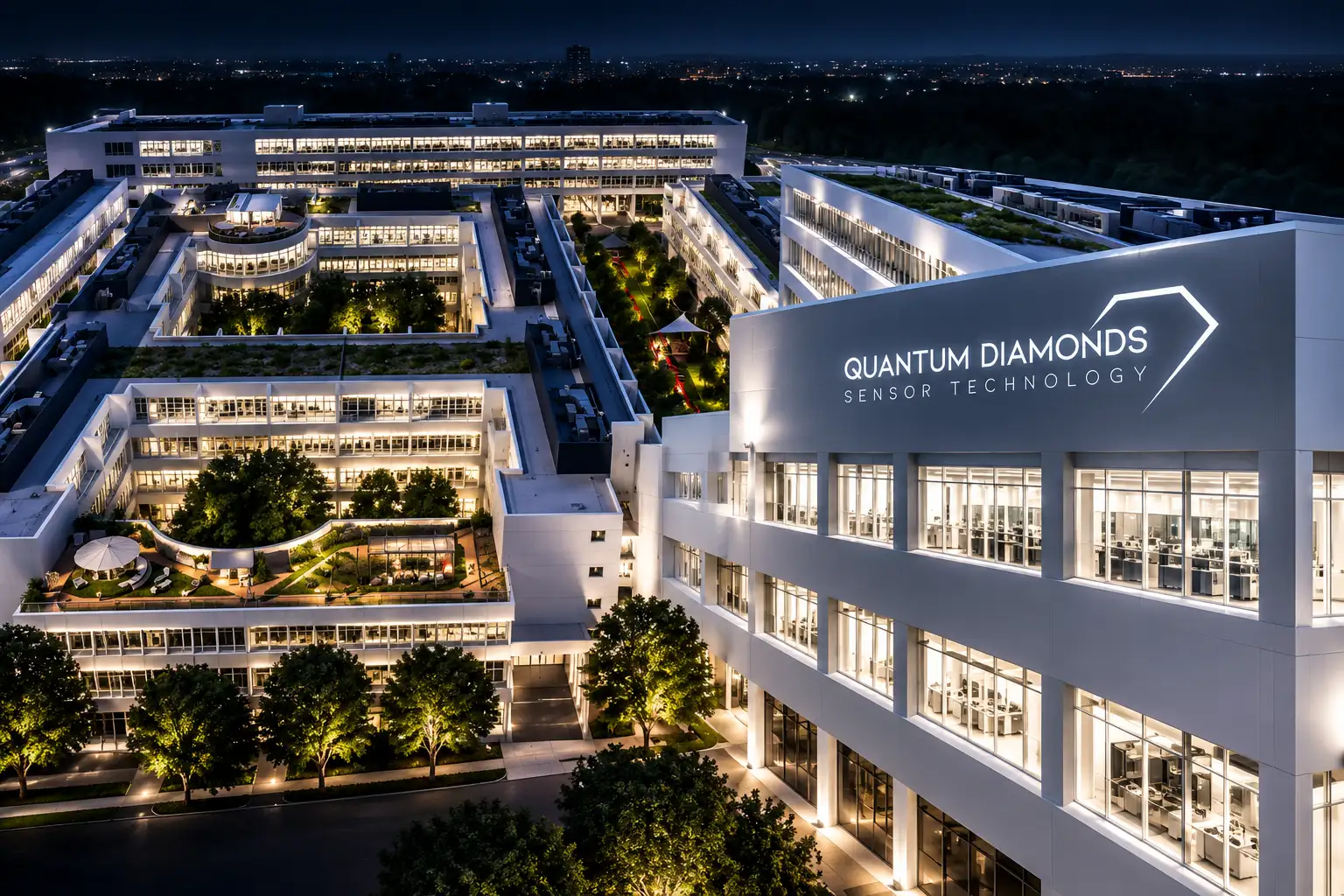
The company’s own page says the first section of the new Munich facility is up and running, brought online on a fast track in just four months. Hubert Aiwanger, Bavarian deputy minister-president and economy minister, and Dr. Irina Kerner of the Federal Ministry for Economic Affairs and Energy toured it on July 23, 2026. They watched a QDm.1 in operation, sat through a live demonstration, and saw early work on full-wafer mapping. The funding decision was handed over on that visit.
Fourteen days earlier, the July 9 statement still said the first operational section was expected later in 2026. The hall opened on the July 23 visit. The December 2025 plan had already named eastern Munich as the site. Aiwanger said then that the location sent a strong signal for microelectronics in the region, and that federal and Bavarian support was an investment in jobs and technological sovereignty.
The hall is not the finished €152 million campus. QuantumDiamonds has described sensor lines for quantum-grade diamond substrates, cleanroom integration of inspection systems, joint labs with chip partners, and support for fab and inline work. The July opening is the first slice, built fast enough to show a working tool to the ministers who signed the cheque.
Stacked Dies Hide Faults Thermal Cameras Cannot See
AI accelerators, high-bandwidth memory, and phone processors now live in 2.5D and 3D stacks. Dies sit on interposers. Current runs through TSVs, microbumps, and chiplets. Once those layers are closed, a short or an open can sit where a thermal camera and an X-ray cannot name it without cutting the part.
Dr. David Su, former director of TSMC’s failure-analysis team and now a QuantumDiamonds advisor, has been blunt about that gap.
Non-destructive fault isolation in advanced packaging is an incredibly difficult challenge that the industry is still working on to solve. This technology shows significant promise in addressing that gap. By detecting magnetic fields to trace current, it offers a potential pathway to visualize defects that are currently invisible to standard thermal or X-ray tools.
Dr. David Su, former TSMC failure-analysis director, QuantumDiamonds advisor
Dr. Fleming Bruckmaier, chief technology officer and co-founder, said the tools give fabs layer-specific insight into current paths in TSVs, microbumps, and chiplets without opening the package, and that this class of inspection is essential once heterogeneous integration is the default. The December plan tied the same problem to AI, mobile, and automotive electronics.
A single percentage point of yield on a high-volume device can be worth millions of dollars a week, the company said, citing industry analysis. That is why independent labs and the large manufacturers have been willing to run proof-of-concept work. It is also why a Munich equipment plant can matter to a Taiwanese or Korean line even if Europe never wafers the part.
How the QDm.1 Sees Current in a Closed Chip
The sensor is a synthetic diamond. Nitrogen-vacancy centres in that crystal change their glow when a magnetic field from a buried current passes through, and the QDm.1 turns those readings into a three-dimensional map of where current is flowing. The scan runs at room temperature and ambient pressure. No vacuum. No sample grind. The diamond head does not have to touch the die.
The commercial unit, the QDm.1, is sold as a failure-analysis microscope for shorts, leakages, and opens at package and die level, including backside power networks and wide-bandgap parts in GaN and SiC. A Tier 1 U.S. chip designer working with the tool said, “We’d been trying to debug this chip for six weeks. You found the defect in under a minute.”
QDM.1 LAB FIGURES
| Metric | Published value |
|---|---|
| Lateral resolution (xy) | Down to 1 μm |
| Depth resolution (z) | Down to 0.5 μm |
| Field of view | Up to 3 mm x 3 mm |
| Stitched area | Up to 5 cm x 5 cm |
| Typical measurement | 5-10 minutes |
The public product page lists lateral resolution down to 1 μm, with depth down to 0.5 μm, a one-shot field up to 3 mm by 3 mm, and automatic stitching out to 5 cm by 5 cm. Typical measurement time is 5-10 minutes. The same page puts the tool on a suspended optical table, on 230 V single-phase power at 16 A, between 15 and 40 °C.
Berghoff has said customers care about the map, not the quantum label. The physics is a means. The job is finding a buried short before a stack is scrapped.
Sunnyvale and Hsinchu Took the First Systems
Proof-of-concept work with 9 of 10 of the world’s largest chip manufacturers was already in the December 2025 announcement, with early systems in Europe and U.S. and Taiwan installs then scheduled for the first quarter of 2026. Those installs landed, but not inside a captive TSMC or Intel bay. They landed in independent failure-analysis houses that serve those clusters.
THE ROAD FROM PLAN TO BENCH
- December 15, 2025: QuantumDiamonds announces the €152 million Munich plant and names expected Chips Act support.
- February 24, 2026: Signs a memorandum with Woowon Technologies at SEMICON Korea for local market work, technical support, and joint customer calls.
- March 2026: Opens a Taiwan hub and names Peter Lemmens, formerly general manager Taiwan at IMS Nanofabrication and imec, as managing director Asia.
- April 8, 2026: Installs the first U.S. QDm.1 at Eurofins EAG Laboratories in Sunnyvale, California.
- April 21, 2026: Installs the first Asia QDm.1 at Integrated Service Technology (iST) in Hsinchu, Taiwan.
- June 23, 2026: Commission clears the €76 million grant.
- July 9, 2026: Closes the €15 million Series A.
- July 23, 2026: Opens the first Munich hall and receives the funding decision on site.
- September 2, 2026: Reports contact-free current imaging as a step toward inline inspection.
Eurofins EAG is a materials and failure-analysis lab in the middle of the Silicon Valley chip trade. iST is one of Asia’s independent test and FA houses, sitting in the Hsinchu cluster. Dr. Sean Shen, director of iST’s failure-analysis engineering division, said his customers work at the leading edge of chip complexity and need tools that keep pace.
The QDm.1 gives our engineers a fundamentally new way to interrogate advanced devices, non-destructively, in three dimensions, and at a speed that fits our workflow. We see significant potential for this technology across the range of advanced packaging and high-density interconnect challenges our customers face.
Dr. Sean Shen, Director of Failure Analysis Engineering, iST
Lemmens called the iST install a defining moment because Hsinchu holds some of the most demanding manufacturing and test operations in the world. Berghoff said Taiwan is the epicenter of advanced semiconductor manufacturing and that the install was validation that quantum sensing is ready for those rooms. Bruckmaier, at the Korea signing, pointed at Samsung and SK Hynix and said the company had already been in contact with several Korean firms and saw strong interest, especially around HBM and advanced memory.
That map is the second-order story in plain geography. Public money holds production in Munich. The first paying benches are next to the lines that actually stack AI packages. The December text quoted an evaluation report saying QuantumDiamonds has the potential to create the next ASML. ASML’s leverage is a tool every advanced fab must buy. The test for this company is whether a diamond microscope follows that path, or stays a specialist FA instrument that fabs call when a part is already in trouble.
Contact-Free Imaging Moves the Tool Toward the Line
The QDm.1 on the market is an in-lab system. The company’s site lists in-lab defect localization as commercially available and in-line wafer mapping as under development. On September 2, 2026, it said it had shown a way to image current without a wired electrical bias, by driving current with microwave fields and reading the same diamond sensor head already shipping in the QDm.1.
Berghoff called that the most important technical milestone on the path to inline electrical inspection, and said manufacturers were already pushing their own samples in front of it. Foundries and packaging customers are evaluating the method on die- and package-level parts. Patent applications have been filed. Throughput for a production line is still the open engineering job.
WHERE THE TOOL STANDS
- In-lab: QDm.1 is shipping for single-chip failure analysis in Europe, the United States, and Asia.
- Contact-free drive: Microwave excitation removes the need for galvanic contacts, the constraint that kept the method in the FA lab.
- In-line: Full-wafer mapping is under development; the July 23 tour included a first look at that work.
- Scale question: A lab microscope still has to match the speed and uptime of the inspection incumbents if it is going onto a packaging line.
Berghoff and Bruckmaier spun the company out of the Technical University of Munich in 2022. Early support came from the EIC Accelerator and SPRIN-D. Mason Sinclair, a partner at IQ Capital, said the firm’s technical pace had been exceptional since a seed investment in late 2023. The July 23 visit also sat beside a separate TUM collaboration, TroDeQu, aimed at detecting hardware trojans with quantum sensing, a research track rather than a product ship date.
Hubert Aiwanger and Irina Kerner walked the Munich hall on July 23, 2026, and watched a QDm.1 run live. The same sensor design was already on the bench at iST in Hsinchu and at Eurofins EAG in Sunnyvale, looking for buried shorts in packages that never get opened.
Frequently Asked Questions
What Power and Lab Setup Does a QDm.1 Need?
The published requirements are 230 V single-phase at 16 A, a suspended optical table with a stabilised sample region, and an operating band of 15 to 40 °C at room pressure. For high-current power devices the scan can finish in a few seconds; leakage work down in the nanoamp range can run from 20 minutes to two hours, which is why the product page quotes 5-10 minutes as typical rather than as a hard cycle time.
Is the QDm.1 a Scanning or a Wide-Field Tool?
It is a wide-field quantum diamond microscope. The diamond is illuminated and read across the whole field at once, up to 3 mm by 3 mm in a single shot, rather than rastering a laser point by point. Larger packages are covered by stitching those fields across a 5 cm by 5 cm travel range without pulling the sample off the stage.
What Extra Duties Come With the German Grant?
Beyond building the Munich site, QuantumDiamonds agreed to take priority orders if supply tightens, open part of the facility to startups and university labs, share upside profits with Germany, and deepen ties with research institutes. It is also seeking Integrated Production Facility recognition, which would lock in further supply and workforce duties under the Chips Act rulebook.
Who Is Peter Lemmens at QuantumDiamonds?
Lemmens is managing director Asia, appointed when the company opened its Taiwan hub in March 2026. He has more than 25 years in semiconductors and electronics, including over 15 years based in Taiwan, a 12-year stretch at Philips, and a prior post as general manager Taiwan at IMS Nanofabrication and imec. The firm hired him to work the Taiwan, Japan, and Korea accounts from Hsinchu rather than from Munich.
What Did the South Korea Deal Cover?
The February 24, 2026 memorandum with Woowon Technologies, signed at SEMICON Korea, set a framework for market development, local technical support, and joint customer engagement. Woowon already represents advanced equipment makers for Korean lines. Bruckmaier used the signing to flag interest from memory houses in a market built around HBM stacks, where TSV and bump yield is a live cost.

UPI MDR Delay Hands Traders the Calendar After Paytm Falls

Google Messages Builds Nine In-Chat Games After Samsung’s Exit

Anthropic’s $100 Million Academy Trains the Firms That Bill Both Sides

Toyota’s Electric C-HR Leaves the Cheap Twin to Subaru

Markets Bet the Fed Skips October After Hawkish Minutes

The Orchard Bug Forced Zcash to Open an Empty Pool

The $5.99 Game That Won Steam’s 2026 Summer Sale

Don Lee Joins Hemsworth as Extraction 3 Starts Shooting

YouTube Shorts Retires Dislikes and Swaps Likes for Hearts

NEURA Robotics Is Spending Its $1.4B on a Machine Stack
-
 NEWS5 months ago
The Orchard Bug Forced Zcash to Open an Empty Pool
-
 GAMING5 months ago
The $5.99 Game That Won Steam’s 2026 Summer Sale
-
 ENTERTAINMENT7 months ago
Don Lee Joins Hemsworth as Extraction 3 Starts Shooting
-
 NEWS4 months ago
YouTube Shorts Retires Dislikes and Swaps Likes for Hearts
-
 NEWS4 months ago
NEURA Robotics Is Spending Its $1.4B on a Machine Stack
-

 NEWS5 months ago
Atlantic City Turned WWE’s Return Into a Civic Night
-

 AUTO6 months ago
Kawasaki Bets the New Z1100 Against Its Own Supercharger
-
 BUSINESS5 months ago
Norway’s Export Bank Backs Nscale’s $790 Million Narvik Loan