
NEWS
Europe’s Photonics Scaleups Quietly Build AI’s Optical Layer
Six EIC Scaling Club photonics firms turn light science into chips, satellite links and metrology as optical interconnect demand surges for AI and sovereignty.

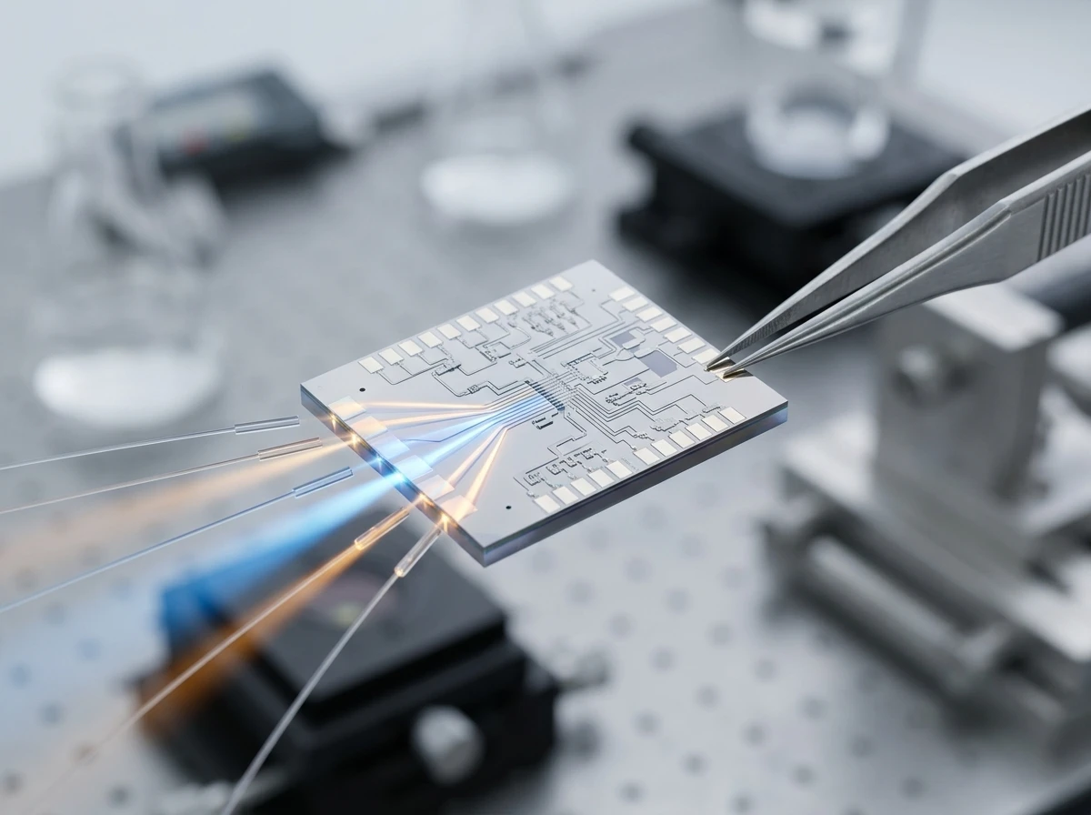
Six European photonics scaleups are commercialising chips, beam shapers and metrology tools that move data with light instead of electricity, cutting power draw and raising bandwidth where copper hits physical walls inside AI clusters and satellite constellations.
They sit inside the EIC Scaling Club and now ride explicit policy recognition in the proposed Chips Act 2.0. The story is less about lab curiosities and more about Europe turning long-held light-science strength into the optical layer AI infrastructure cannot scale without.
Copper Hits Its Limit Inside AI Racks
AI training clusters pack tens or hundreds of thousands of GPUs. Electrical interconnects generate heat, burn watts and struggle with latency at the distances and densities required. Optical links using lasers, modulators and photodetectors deliver higher bandwidth at lower energy per bit.
Market trackers put the broader optical interconnect market near $17.9 billion in 2025, with forecasts climbing past $60 billion by the mid-2030s at mid-teens CAGRs. AI-specific optical interconnect segments show even steeper curves, with some projections from roughly $8.6 billion in 2025 toward $38 billion by 2034.
- Silicon photonics alone is tracked growing at 23-28% CAGR into the early 2030s as data-centre modules shift from discrete optics to integrated platforms.
- Co-packaged optics and in-package optical I/O remain early but show the steepest growth paths as switch ASICs and accelerators demand closer photonic I/O.
- Europe’s share of optical production has slipped, yet R&D spend and specialised component makers remain dense across the Netherlands, France, Germany, Spain and Ireland.
That demand surge is exactly where the scaleups operate. Copper still moves short-reach traffic inside many racks, yet the heat and wattage penalties climb as GPU counts rise and links stretch across rows and buildings. Light sidesteps those physical walls by carrying more bits per joule once the lasers, modulators and detectors sit close enough to the silicon.
The steeper AI-specific curve versus the broader interconnect market shows where capital is concentrating. Hyperscalers and sovereign compute projects need the energy-per-bit gains first. That pull reaches back into the component makers, the packaging houses and the metrology tools that keep advanced packages on yield.
Six Firms Mapping Light Across Networks and Fabs
The companies span coherent lasers for telecom and data-centre edge, free-space optical terminals for space, wafer metrology for advanced packaging, quantum randomness for security, and selective solar glass for greenhouses. All are EIC Scaling Club members.
| Company | Country | Core focus | Notable capital |
|---|---|---|---|
| EFFECT Photonics | Netherlands | Integrated InP coherent lasers and PICs for telecom/DCI | Series D extended to $62M; ~$174M total raised |
| Cailabs | France | Multi-Plane Light Conversion beam shaping for satellite, fibre and industrial lasers | €57M industrial scale-up round |
| Wooptix | Spain | Wavefront Phase Imaging wafer metrology (Phemet) | Over €10M Series C (Samsung Venture led) |
| Mbryonics | Ireland | Free-space optical terminals and PICs for satellites | EIC-backed deep-tech trajectory |
| Quside | Spain | Quantum random number generators and single-photon sources | Integrated photonics quantum hardware |
| Brite Solar | Greece | Transparent PV glass that transmits crop-useful wavelengths | Photonics + materials for agri-energy |
EFFECT Photonics, spun from Eindhoven University of Technology, builds monolithic InP photonic integrated chips that combine lasers, modulators and detectors. Its pico ITLA form factor is more than 50% smaller than typical nano units and targets 100G ZR pluggables; a higher-power nano version aims at 400/800G coherent links. The company holds 91 granted patents and runs a fabless model with European design roots.
Cailabs uses Multi-Plane Light Conversion to shape laser beams for higher-capacity fibre links, optical ground stations and precise industrial welding or additive manufacturing. Its September 2025 €57M raise funds production scale and global reach.
Wooptix applies astronomy-derived adaptive optics to semiconductor wafers. Its Phemet system captures over 16 million data points in a single shot for shape, nanotopography and roughness at sub-nanometer height resolution. The firm closed over €10 million Series C led by Samsung Venture Investment Corporation and SETT, with Intel Capital and the EIC Fund among backers. It has installed its first system at CEA-Leti and is building cleanroom capacity in Spain.
Mbryonics packs optical terminals and laser payloads into compact photonic integrated circuits so satellites can move far more data than radio-frequency systems allow, with lower size, weight and power. Quside generates true quantum randomness for encryption and supplies single-photon sources for quantum computing and sensing. Brite Solar coats greenhouse glass to pass photosynthetically active light while converting the rest into electricity, cutting energy costs without yield loss.
Together the six cover distinct layers of the same shift. Coherent lasers and beam shapers attack bandwidth and reach. Free-space terminals open space links that radio cannot match on throughput. Metrology keeps the packages that hold those optics on yield. Quantum sources harden the security layer. Selective glass extends photonics into energy and food production. The common thread is moving or measuring light where electricity or radio hits a wall.
Policy Finally Names Photonics Inside the Chips Framework
Photonics21 welcomed the European Commission’s July 2026 proposal to place photonics and integrated photonics explicitly inside Chips Act 2.0. The platform argues future semiconductor competitiveness rests on bandwidth, energy efficiency and advanced packaging, areas where co-integrating photonic and electronic chips delivers decisive gains.
Photonics already underpins roughly 20% of the EU economy across healthcare, manufacturing, telecoms, defence and quantum. The industry group wants semiconductor-related photonics fully inside the Chips Joint Undertaking while a separate ring-fenced partnership covers the wider ecosystem of lasers, biophotonics and free-space optics.
The original European Chips Act sovereignty goals aim to double Europe’s global semiconductor market share. Adding photonics aligns that ambition with AI interconnect, secure satellite links and advanced packaging metrology. Pilot lines such as PIXEurope already target photonic chip manufacturing under the Chips JU.
The same firms appear inside the EIC Scaling Club community of 120 scale-ups, which reports strong funding growth among members and pairs them with investors and corporates. That combination of targeted public capital and private rounds is what turns university spin-outs into production suppliers.
Naming photonics inside the chips framework matters because it ties optical I/O and co-packaged designs to the same sovereignty goals that already cover logic and memory. Without that link, interconnect remains an afterthought even as AI clusters choke on copper. With it, pilot lines, design support and qualification paths can treat the photonic layer as core infrastructure rather than a side specialty.
Where the Money and Demand Flow
Optical interconnect and silicon photonics numbers show the pull from hyperscalers and sovereign compute projects. Europe’s data-centre buildout, driven by AI strategy and sustainability rules that favour lower-power optics over copper, is one regional driver. Satellite constellations and defence optical links form another.
| Segment | Recent size marker | Projected growth |
|---|---|---|
| Optical interconnect (broad) | ~$17-18B (2025/26) | 12-14% CAGR into early 2030s |
| Optical interconnect for AI | ~$8.6B (2025) | ~18% CAGR toward $38B by 2034 |
| Silicon photonics | ~$2.8-3.6B range (2025/26) | 23-28% CAGR |
Public markets already price the theme aggressively: Lumentum, Coherent and specialist names have posted triple-digit moves on AI networking orders and co-packaged optics backlogs. European equipment and materials names that supply MOCVD tools for InP lasers, photonics-SOI wafers and process metrology trade at discounts to US peers yet sit upstream of the same boom. Crowd discussion on X repeatedly flags that German and French toolmakers hold outsized leverage most US-centric investors overlook.
Scaleups such as EFFECT and Cailabs sell into the same hyperscaler and telecom supply chains. Wooptix sells yield and process control into the fabs that must produce the advanced packages those optics sit inside. The European layer is therefore both component and enabler.
The split between broad interconnect growth and the steeper AI and silicon-photonics curves explains why private rounds and EIC capital are landing now. Buyers are no longer waiting for lab demos. They are qualifying form factors, beam-shaping modules and metrology tools against roadmaps already locked for 800G and beyond.
Who Benefits When Light Replaces Wire
Hyperscalers gain denser, cooler racks and lower operating power. Telecom operators get smaller, cheaper coherent pluggables for edge and metro. Satellite operators unlock higher-throughput, more secure links that radio cannot match. Chipmakers using Wooptix-style metrology improve yields on 3D integration and advanced packaging, the exact architectures AI accelerators require.
Downstream European winners include:
- Data-centre operators facing carbon and power constraints who can swap copper for photonics to hit PUE targets.
- Defence and dual-use programmes that need resilient free-space optical links and quantum-secure randomness.
- Greenhouse operators and agri-tech firms that turn roof glass into dual-use energy generators without starving crops of light.
- Adjacent European optical startups, including those closing rounds for AI optical interconnect pre-seed round activity and larger optical bet against Nvidia chips valuations that signal investor appetite for the broader theme.
Losers are slower copper-centric interconnect suppliers and any European fab strategy that ignores photonic co-integration. The second-order effect is talent and capital concentration: Eindhoven, Rennes, Madrid, Galway and related clusters become harder to ignore when the products ship.
The benefit map is uneven by design. Operators under the tightest power and carbon limits feel the optics advantage first. Satellite and defence buyers pay for performance and security premiums that radio cannot deliver. Fab engineers chasing yield on advanced packages need metrology that can resolve sub-nanometer topography in a single shot. Each group pulls a different firm in the cohort, yet all of them reinforce the same industrial base.
Funding Milestones Show The Scale Path
Recent capital and customer steps already sketch how the cohort moves from design strength toward volume supply. The dates and figures sit in the public record of the same six firms and the policy track that now names their technology.
- Series D extension to $62M for EFFECT Photonics, lifting total capital raised to roughly $174M and backing the pico ITLA push into 100G ZR and higher-power 400/800G coherent links.
- September 2025 €57M industrial scale-up round for Cailabs, earmarked for production capacity and global reach across fibre, satellite ground stations and industrial laser markets.
- Over €10M Series C for Wooptix, led by Samsung Venture Investment Corporation and SETT, with Intel Capital and the EIC Fund among backers, followed by a first system install at CEA-Leti and cleanroom buildout in Spain.
- July 2026 Commission proposal placing photonics and integrated photonics explicitly inside Chips Act 2.0, the policy step Photonics21 welcomed as recognition that bandwidth and packaging now define semiconductor competitiveness.
Those steps do not guarantee high-volume wins. They do show capital, customer access and policy alignment arriving in the same window. Fabless InP design, beam-shaping production lines and wafer metrology on a leading research fab floor are concrete rather than aspirational markers. The remaining gap is the cost and qualification curve that hyperscalers demand at 800G and 1.6T.
Clusters Turn Research Strength Into Supply
Europe’s photonics edge has long lived in materials, design tools and specialised process steps rather than in high-volume commodity optics. The scaleups convert that edge into shippable product by staying close to the universities and pilot lines that trained their founders and staff.
Eindhoven anchors the InP coherent work behind EFFECT. French industrial photonics capacity supports Cailabs’ Multi-Plane Light Conversion platforms. Spanish cleanroom investment and the CEA-Leti install give Wooptix a path from astronomy-derived imaging into fab-floor metrology. Irish deep-tech support backs Mbryonics’ compact free-space terminals. Spanish integrated-photonics work underpins Quside’s quantum sources. Greek materials expertise feeds Brite Solar’s selective greenhouse glass.
Dense R&D spend across the Netherlands, France, Germany, Spain and Ireland keeps the specialised component base alive even after Europe’s share of broader optical production slipped. When policy names photonics inside the chips framework and EIC vehicles pair the same firms with investors and corporates, those clusters gain a clearer route from prototype to qualified supply. Talent and follow-on capital then have a reason to stay rather than migrate to larger US or Asian hubs.
The Sovereignty Test Is Commercialisation Speed
Europe already leads in many photonic materials, design tools and specialised manufacturing steps. The open question is whether the scaleups can reach high-volume, high-reliability production before US and Asian competitors lock the AI optical supply chain.
EFFECT’s fabless InP platform and pico form-factor push are early commercial answers. Cailabs’ industrial raise funds capacity. Wooptix’s Samsung-backed metrology and CEA-Leti install put a European tool on the factory floor. Mbryonics and Quside target niches (space optical terminals, quantum hardware) where performance and security premiums justify European supply.
Policy now names the technology. Capital is arriving through EIC vehicles and private rounds. The remaining work is execution: yield, packaging, customer qualification and cost curves that match hyperscaler roadmaps for 800G and 1.6T generations.
If those pieces lock, Europe’s photonics cohort stops being a research strength story and becomes a durable industrial one. The light layer for the next decade of compute and connectivity will have a clear European stamp on it.


OpenAI Bets $300 Donut Speaker Can Seed Its Device Future

OpenAI Bets $300 Donut Speaker Can Seed Its Device Future

Dell Parks Flagship XPS 13 Chassis on Googlebook Platform

OpenAI Bets $300 Donut Speaker Can Seed Its Device Future

CLARITY Act Delay Leaves Crypto Bill Racing a Midterm Clock

Ethics Deal on CLARITY Act Could Force Trump Crypto Sale With Tax Deferral

Chrome Wins Netflix 4K on Windows 11 but Edge Keeps More

Tight Jobless Claims Cap Bitcoin Under $65,000 on Hike Odds

Maher Gasps at DSA Communists While Hollywood Stays Silent

Netflix Gets GTA 6 Extended Look Six Hours Before YouTube

Fed Minutes Cite AI Demand as Inflation Risk, Put a 2026 Hike Back on the Map

Marker AI Writing Startup Lands $13M Seed Led by Index Ventures

Meta’s Muse Spark 1.1 Beats Rivals on Price, Trails on Coding

Finto Picks Munich Over Silicon Valley After YC, Raises $3.4M

CS2 Premier Season 5 Lands With Cache and a C4 Damage Rework

Backrooms Returns to Theaters as the Everything Must Go Edition

Trump Calls Iran ‘Islamic Republic of Japan’ as Ceasefire Ends

IO Interactive Regains Project Fantasy, Closes Istanbul Studio

Kord’s £6.4M Series A Bets Identity and Payments Run on One Stack

Taiwan Margin Debt Climbs 160% as Locals Borrow Into the TSMC Rally
-
 FINANCE2 months ago
Zcash Patched a Double-Spend Bug as ZEC Climbed 5%
-
 ENTERTAINMENT2 months ago
Steam Summer Sale 2026 Locks In June 25 to July 9 Dates
-

 FINANCE1 month ago
CLARITY Act Final Text Expected This Weekend as 60-Vote Hurdle Looms
-
 NEWS3 months ago
Meta Adds AI Replies to Threads, But Users Can’t Block It
-
 ENTERTAINMENT3 months ago
‘Widow’s Bay’ Review: Apple TV’s Sleeper Horror-Comedy Earns Its Fog
-
 NEWS5 months ago
U.S. Navy Deploys Solar-Powered Lightfish Drone to Patrol Oceans
-
 FINANCE2 months ago
CLARITY Act Floor Vote Likely Shifts to August, Lummis Says
-

 FINANCE1 month ago
Kalshi Loses Major NY Prediction Markets Ruling to Judge Torres